Rekha Verma
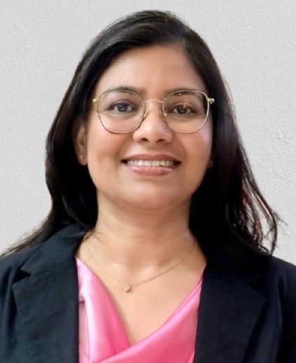
Indian Institute of Information Technology Allahabad,
Prayagraj (UP)- 211 015
Educational Qualification:
- B. E. (Electronics and Communication Engineering), MCET Laxmangarh, University of Rajasthan, 2003.
- M. Tech. (VLSI Design), Banasthali Vidyapith, Banasthali, 2009.
- Ph. D. (DESE), Indian Institute of Science Bangalore, 2013.
Teaching:
Courses taught to UG/PG stuents
- Digital Logic Design with Verilog (U.G.)
- Analog Electronics (U.G.)
- Digital IC Design (U.G.)
- Fundamentals of Electrical and Electronics Engineering (U.G.)
- VLSI Technology/IC Technology
- Modeling of Semiconductor Devices (P.G.)
- Solid State Devices (P.G.)
- Physics of Nanoscale Devices (P.G.)
Introduction to Microelectronics (P.G.)
Research Interests:
Computational Nanoelectronics: Materials and device research for next-generation CMOS/beyond-CMOS transistors, optoelectronic devices, nanoscale interconnect performance & reliability.
Sponsored Research projects
“Silicon Nanowires: Professional Compact Model of Scaled Thermoelectric Figure of Merit for Energy Harvesting”, Young Scientist Award, SERB, Govt. of India, 2016-2019, INR 21,09,800, Role: PI, Status: Completed.
“Ab-initio linear and non-linear ultrafast spectroscopy in two-dimensional nitrogen based binary buckled group V semiconductors”, funded by Indo-Czech International Bilateral Project Govt. of India, (Duration: 2021-2024) INR 1.2 Crores (both sides), Role: Co-PI, Status: Completed.
“Science Technology and Innovation Hub in Information and Communication Technology (ICT) at Indian Institute of Information Technology Allahabad (IIITA), Prayagraj Block, Prayagraj District, Uttar Pradesh State”, funded by the Department of Science & Technology, Govt. of India, (Duration: 2022-2024), ~ INR 1.87 Crores, Role: Co-PI, Status: Completed.
Erasmus+ Programme for Mobility of higher education students and staff between University of Ostrava (UO) and IIIT Allahabad, (Duration: October 2025- September 2027 +1), co-funded by European Union, Role: Departmental Coordinator, Status: Ongoing.
Publications:
(a) Patents:
- R. Verma, S. Bhattacharya and S. Mahapatra, “A graphene based thermoelectric generator”, Indian Patent No. 404071, granted on 22/08/2022.
A. Prabhakar, R. Verma, J. Chauhan, P. Kumari, S. K. Babu Degala, “System for automated medication management and remote monitoring via smart pill dispensing”, Indian Patent No:581981, granted on 27/02/2026.
(b) International Journals
- R. Saraswat, R. VERMA and S. Bhattacharya, "Strain-induced activation of symmetry-forbidden exciton-phonon couplings for enhanced phonon-assisted photo-luminescence in MoS2 monolayers", APS: Physical Review B, 111, 205131 (1-12), 2025.
- P. Sinha, R. VERMA and P.K. Tiwari, "Hydrogen Sulfide‑Based Double‑Gate Single‑Electron Transistor for Charge Detection and Switching Applications", Springer: Journal of Electronic Materials, 54, 792–799, 2025.
- R. Saraswat, M. Kolos, R. VERMA, F. Karlický and S. Bhattacharya, "Phonon Assisted Exciton Processes in Two-Dimensional Tungsten Monocarbide", ACS: Journal of Physical Chemistry C, 128, 8341 -8350, 2024.
- N. Gupta and R. VERMA, "Effect of electron–phonon coupling on transport properties of monolayer germanene: A thermoelectric perspective", Elsevier: Materials Science in Semiconductor Processing, 153, 107115, 2022.
- M. Kolos, L. Cigarini, R. VERMA, F. Karlicky, and S. Bhattacharya, "Large Exciton-Driven Linear and Nonlinear Optical Processes in Monolayers of Nitrogen Arsenide and Nitrogen Antimonide", ACS: Journal of Physical Chemistry C, 126, 14931 –14959, 2022.
- M. Kolos, L. Cigarini, R. VERMA, F. Karlicky, and S. Bhattacharya, "Giant linear and nonlinear excitonic responses in an atomically thin indirect semiconductor nitrogen phosphide NP", ACS: Journal of Physical Chemistry C, 125, 12738 –12757, 2021.
- N. Gupta and R. VERMA, "Thermoelectric Performance of Silicene under Uniform Biaxial strain: A first Principles study", Elsevier: Superlattices and Microstructures", 156, 106944 -106954, 2021.
- N. Gupta and R. VERMA, "First-principles study of thermoelectric transport properties in low-buckled monolayer silicene", Elsevier: Physica B: Condensed Matter", 606, 412715 -412722, 2021.
- R. VERMA, S. Bhattacharya and S. Mahapatra, "Solution of Time Dependent Joule Heat Equation for a Graphene Sheet under Thomson Effect", IEEE Transactions on Electron Devices, 60 , 3548 -3554, 2013.
- R. VERMA, S. Bhattacharya and S. Mahapatra, "Modeling of Temperature and Field Dependent Electron Mobility in a Single Layer Graphene Sheet", IEEE Transactions on Electron Devices, 60, 2695 -2698, 2013.
- R. VERMA, S. Bhattacharya and S. Mahapatra, "Thermoelectric Performance of a Single Layer Graphene Sheet for Energy Harvesting", IEEE Transactions on Electron Devices, 60, 2064 -2070, 2013.
- R. VERMA, S. Bhattacharya and S. Mahapatra, "Physics-Based Solution for Electrical Resistance of Graphene under Self-Heating Effect", IEEE Transactions on Electron Devices, 60,502-505, 2013.
- R. VERMA, S. Bhattacharya and S. Mahapatra, "A physics-based flexural phonon-dependent thermal conductivity model for single layer graphene", Journal of Semiconductor Science and Technology, IOP, 28, 015009 (1)-(6), 2013.
- R. VERMA, S. Bhattacharya and S. Mahapatra, "Theoretical Estimation of Electro-migration in Metallic Carbon Nanotubes Considering Self-Heating-Effect", IEEE Transactions on Electron Devices, 59, 2476 -2482, 2012.
- R. VERMA, S. Bhattacharya and S. Mahapatra, "Analytical Solution of Joule Heating Equation for Metallic Single Walled Carbon Nanotube Interconnects", IEEE Transactions on Electron Devices, 58, 3991-3996, 2011.
(c) International Conferences/Workshops/Symposium, etc. :
- M. Ansari, R. Verma and S. Bhattacharya, “Group theoretic analysis for absence of Phonon assisted sidebands in monolayer MoS2”, 7th International Conference on Emerging Electronics (ICEE 2025), Bengaluru, India to be held during December 13–16, 2025 organized by IEEE EDS.
- R. Saraswat, S. Bhattacharya and R. Verma, “Enhanced Phonon assisted Photoluminescence in monolayer MoS2 under strain”, 7th International Conference on Emerging Electronics (ICEE 2025), Bengaluru, India to be held during December 13–16, 2025 organized by IEEE EDS.
- T. Sharma, R. Saraswat, S. Bhattacharya and R. Verma, “Electronic and hole mobilities in wide band-gap monolayer tungsten carbide”, 8th IEEE Electron Devices Technology Manufacturing Conference (EDTM), Benguluru-India, 2024.
- Rekha Verma, IEEE -EDS Workshop on Devices and Circuits, March 24-26, 2022 organized by the EDS UP chapter and IT Kanpur at Goa, India.
- Rekha Verma, 3rd Virtual Congress on Materials Science and Engineering, September 27th -1st October, 2021.
- Rekha Verma, “Strain Engineering in Tuning the Electronic and Vibrational Properties in Silicene and other 2D Materials” Indo-Polish International Conference, Advances in Energy Harvesting Technology, March 18-20, 2021 (Virtual mode).
- Aayush Khatri, Neelesh Gupta and Rekha Verma, “Investigation of Orientation and Dimension Dependent Thermoelectric Properties of Intrinsic Silicon Nanowire”, 39th International Conference on Thermoelectrics 2020, June 28-July 2, 2020, University of Washington, Seattle, USA.
- Neelesh Gupta and Rekha Verma, “First Principles Analysis of Power Factor in Silicene with Biaxial Strain”, 39th International Conference on Thermoelectrics 2020, June 28-July 2, 2020, University of Washington, Seattle, USA.
- Neelesh Gupta and Rekha Verma, “First Principles Based Exploration of Transport Properties of Monolayer Germanene”, 20th International Workshop on The Physics of Semiconductor Devices (IWPSD-2019), December 17-20, 2019, S. N. Bose National Centre for Basic Sciences, Kolkata, India.
- Rekha Verma, “Ab-initio Study of Lattice Anhamonicities in Bulk Lonsdaleite: Hexagonal Diamond”, 38th International Conference on Thermoelectrics and 4th Asian Conference on Thermoelectrics 2019, June 30-July 4, 2019, Gyeongju, Korea.
- Suchitra Kumari and Rekha Verma, “Self-Energy Corrections of Electrical Conductivity in Silicon Nanowire”, 36th International Conference on Thermoelectrics 2017, July 30 - August 3, 2017, Pasadena, California.
- Rekha Verma, “Graphene based in-chip thermoelectric generator for Nanoscaled devices”, 9th Indo-German Frontiers of Engineering Symposium 2017 March 9-12, 2017, Jaipur, India, co-organized by the DST, Govt. of India and the Alexander von Humboldt Foundation, Germany.
- Rekha Verma, Sitangshu Bhattacharya and Santanu Mahapatra, “Electro-thermal Aspects in Carbon Based Interconnects”, TechConnect World, Summit and Showcase 2013, Nanotech Conference and Expo 2013, May13-16, 2013, Washington DC, USA.
- Rekha Verma and Santanu Mahapatra, “Electro-thermal modeling in Metallic Single Walled Carbon Nanotube Interconnects”, MOS-AK/GSA India 2012, International Workshop on Device Modeling for Microsystems, 2012 , India.
Research Supervision:
PhD: 01 completed in 2022 as Sole Supervisor and 01 ongoing
MTech: 09 completed, 01 ongoing
Professional Recognition & Assignments/ Award/ Prize/ Certificate, Fellowship received
(a) Professional recognition & Assignments:
- Participant (by invitation) at the Indo-German Workshop on Thermoelectric devices for Emerging Applications (IG-WTEA) 2024, fully sponsored Indo-German Science and Technology Centre, GoI during February 26-28, 2024 at IISER Trivandrum.
- Participant (by invitation) at 9th Indo-German Frontiers of Engineering Symposium (INDOGFOE 2017) , from DST, GoI and the Alexander von Humboldt Foundation, Germany during March 9-12, 2017, Jaipur.
- Featured on the homepage of Department of Physics, University of Ostrava, Czech Republic for collaborative research work (https://prf.osu.eu/kfy/30797/joint-successes-of-physicists-from-ostrava-and-indian-allahabad/)
- Vice-chair, IEEE Electron Devices Society (EDS) UP chapter-India from April 2016 – March 2019.
- Board Member -interview board of Kishore Vaigyanik Protsahan Yojana (KVPY) funded by DST, Government of India, during 2015-2020 at Harish-Chandra Research Institute Allahabad-India.
- Reviewer- Royal Society of Chemistry: PCCP, IEEE-Transactions on Electron Devices, IEEE Transactions on Nanotechnology, IEEE TVLSI, IET Electronic Letters, various international conferences.
- Organizing Chair (Special Tracks) for International Conference on Information Communication Technology (CICT), December 6-8, 2023 at IIIT Allahabad.
- Organizer and Chair, Indo-Polish International Conference, Advances in Energy Harvesting Technology, March 18-20, 2021 (Virtual mode), for the track Thermoelectric energy harvesting.
- Invited Speaker at the XXIII International Workshop on Physics of Semiconductor Devices (IWPSD 2025), Roorkee, India organized by IIT Roorkee and SSPL New Delhi, December 16–18, 2025.
- Invited Speaker at the 7th International Conference on Emerging Electronics (ICEE 2025), Bengaluru, India organized by IEEE EDS, December 13–16, 2025.
- Resource person at the AICTE QIP PG Certification Program (SemChips) organized by IIIT Allahabad during July 1-12, 2025.
- Invited Speaker at the IEEE-EDS Workshop on Devices and Circuits, organized IEEE UP section and IIT Kanpur, January 23-27, 2026, Jaisalmer- India.
- Invited Speaker at the IEEE-EDS Workshop on Devices and Circuits, organized IEEE UP section and IIT Kanpur, January 17-21, 2025, Goa-India.
- Invited Speaker at the IEEE-EDS Workshop on Semiconductors, organized IEEE UP section and IIT Kanpur, August 17-21,2025, Mussoorie- India.
- Invited Speaker at IEEE-EDS Workshop on Devices and Circuits Organized by IIT Kanpur and IIT Jammu, June 11-15, 2024, Srinagar- India.
- Invited talk, “Ab‐initio Studies of Transport Properties of Monolayer hexagonal 2D materials for Thermoelectric Applications”, at University of Ostrava, Czech Republic during R&D visit from 15/09/2023 to 01/10/2023.
- Invited speaker at the IEEE-EDS Workshop on Devices and Circuits (WDC) 2023, Khajurao, India during January 26-28, 2023 organized by IEEE EDS UP and MP Chapters.
- Invited speaker at the 6th World Congress on Materials Science and Engineering, Rome-Italy during September 18-19,2023 for the theme “Outlining the Importance of Materials Science for a Better Future.
- Invited Speaker at IEEE-EDS Workshop on Devices and Circuits Organized by IEEE UP and IIT Kanpur, March 24-26, 2022, Goa.
(b) Awards/Fellowships received:
- Prestigious “TechnoInventor Award 2014” from India Electronics and Semiconductor Association (IESA) for outstanding research contribution in PhD work.
- MHRD, GoI Fellowship at Indian Institute of Science, Bangalore-India during August 2011-April 2014.
- International Travel Grant 2013 from DST and CSIR, Government of India for presenting paper in International conference.
- Microsoft Research grants 2013 from the Electrical Sciences division of Indian Institute of Science, Bangalore.
- International Travel Support 2013 under GARP-Deputations from the Indian Institute of Science, Bangalore.
- Fellowship from DST, GoI at Indian Institute of Science, Bangalore during August 2010-July 2011.
- Fellowship from R&D cell at Indian Institute of Technology Kanpur-India for working on the project entitled “Solar Energy Research Enclave” during February 2010-July 2010.
- पिछले पृष्ठ पर वापस जाएं
- |
-
पृष्ठ अंतिम बार अद्यतन तिथि:13-08-2026 12:51 PM